
Delve into the Intricate Realm of Semiconductor Heterostructures and Nanostructures: A Comprehensive Guide

In the rapidly evolving field of electronics, semiconductor heterostructures and nanostructures have emerged as game-changing technologies, enabling groundbreaking advancements in device performance and functionality. This comprehensive book, Characterization of Semiconductor Heterostructures and Nanostructures, provides an in-depth exploration of these fascinating structures, empowering researchers, engineers, and students with the knowledge and techniques necessary to harness their extraordinary potential.
Unveiling the Fundamentals
The book begins by laying a solid foundation in the basic principles underlying heterostructures and nanostructures. It elucidates the concepts of bandgap engineering, quantum confinement, and carrier transport, providing a clear understanding of the unique electronic and optical properties that these structures exhibit.
4.2 out of 5
| Language | : | English |
| File size | : | 14564 KB |
| Text-to-Speech | : | Enabled |
| Screen Reader | : | Supported |
| Enhanced typesetting | : | Enabled |
| Print length | : | 496 pages |
| X-Ray for textbooks | : | Enabled |
A Comprehensive Toolbox
The heart of the book lies in its thorough examination of characterization techniques. Readers embark on a guided tour of the most cutting-edge methods employed to probe the structural, electrical, and optical characteristics of heterostructures and nanostructures. These techniques include:
* 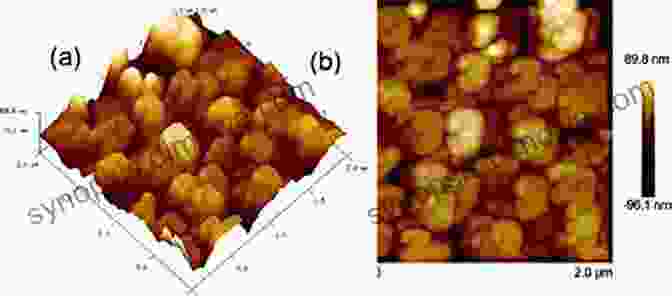 Atomic Force Microscopy (AFM) * Transmission Electron Microscopy (TEM) * Scanning Tunneling Microscopy (STM) * Photoluminescence Spectroscopy (PL) * Raman Spectroscopy
Detailed descriptions, practical examples, and illustrative figures ensure that readers gain a profound understanding of each technique's capabilities and limitations.
Practical Applications
The book seamlessly bridges the gap between theoretical understanding and practical applications. It showcases the real-world relevance of heterostructures and nanostructures in a myriad of cutting-edge technologies:
* High-efficiency solar cells * Ultra-fast lasers * Advanced transistor designs * Quantum computing * Medical imaging
Through real-world case studies and insightful discussions, readers witness firsthand how these transformative materials are shaping the future of electronics and beyond.
Cutting-Edge Research
Beyond established characterization techniques, the book delves into the latest advancements at the forefront of research. Readers are exposed to emerging methodologies, such as:
* Time-resolved photoluminescence * Magneto-optical spectroscopy * Nanoscale scanning probe techniques
By providing a glimpse into the cutting edge of the field, the book prepares readers to contribute meaningfully to future innovations in semiconductor heterostructures and nanostructures.
Pedagogical Excellence
The book is crafted with pedagogical excellence in mind. Each chapter features:
* Clearly defined learning objectives * Thought-provoking exercises and review questions * Comprehensive references for further exploration
This structured approach ensures that readers retain and fully grasp the complex concepts presented throughout the book.
Characterization of Semiconductor Heterostructures and Nanostructures is an indispensable resource for anyone seeking a comprehensive understanding of these transformative materials. Its in-depth coverage, practical examples, and cutting-edge insights empower readers to harness the full potential of heterostructures and nanostructures for groundbreaking advancements in electronics and beyond.
Free Download your copy today and embark on an enthralling journey into the intricate and fascinating world of semiconductor heterostructures and nanostructures.
4.2 out of 5
| Language | : | English |
| File size | : | 14564 KB |
| Text-to-Speech | : | Enabled |
| Screen Reader | : | Supported |
| Enhanced typesetting | : | Enabled |
| Print length | : | 496 pages |
| X-Ray for textbooks | : | Enabled |
Do you want to contribute by writing guest posts on this blog?
Please contact us and send us a resume of previous articles that you have written.
 Book
Book Novel
Novel Page
Page Chapter
 Text
Text Story
Story Genre
Genre Reader
 Library
 Paperback
 E-book
 Magazine
 Newspaper
 Paragraph
 Sentence
 Bookmark
 Shelf
Shelf Glossary
 Bibliography
 Foreword
 Preface
 Synopsis
 Annotation
 Footnote
 Manuscript
 Scroll
 Codex
Codex Tome
Tome Bestseller
 Classics
 Library card
 Narrative
 Biography
 Autobiography
 Memoir
 Reference
 Encyclopedia
 David Shiffman
 David Barrett
 David S Walls
 David Podlipny
 David L Price
 David Pitt Brooke
 David Almond
 David Simchi Levi
 Helen Moss
 David Faulkner
 Kazune Kawahara
 Deca
Deca Mark Phillips
 David Snider
 Deborah Ruddell
 David Castle
 David Gordon Wilson
 David D Cox
 David Grote
 Deepak Mahajan
Light bulbAdvertise smarter! Our strategic ad space ensures maximum exposure. Reserve your spot today!


 Leslie CarterDive into the World of Bisimulation and Coinduction: An In-depth Exploration
 George MartinMoon Sun Picture Circle For Children Circle Stories: A Journey of Wonder and...
 Herman MitchellFollow ·16.3k
 Brian BellFollow ·17.1k
 Jamal BlairFollow ·8k
 Kyle PowellFollow ·13.6k
 Robin PowellFollow ·10.9k
 Gage HayesFollow ·2.1k
 Ken SimmonsFollow ·8.2k
 Chris ColemanFollow ·5k

 Aron Cox
Mastering Project Management: The Ultimate Guide to...
In today's competitive...

 Dominic Simmons
Let's Build Sue Fliess: Unleash the Polychrome Master...
Chapter 1: The...

 Mason Powell
Master the Digital Marketing Landscape: Fundamentals of...
In the age of digital...

 Aubrey Blair
Uncover the Secrets of Ancient Blades and Enchanting...
Embark on an Enchanting Journey into the...

 Shannon Simmons
Unleash the Spooktacular with Spooky Crochet Tutorials...
Prepare to be spooked...

 Cade Simmons
Immerse Your Little Ones in a World of Enchantment with...
Nursery rhymes have forever ignited the...
4.2 out of 5
| Language | : | English |
| File size | : | 14564 KB |
| Text-to-Speech | : | Enabled |
| Screen Reader | : | Supported |
| Enhanced typesetting | : | Enabled |
| Print length | : | 496 pages |
| X-Ray for textbooks | : | Enabled |
